- 您现在的位置:买卖IC网 > Sheet目录3879 > PIC24F08KL401-I/SS (Microchip Technology)IC MCU 16BIT 8KB FLASH 20-SSOP
PIC24F16KL402 FAMILY
DS31037B-page 14
2011 Microchip Technology Inc.
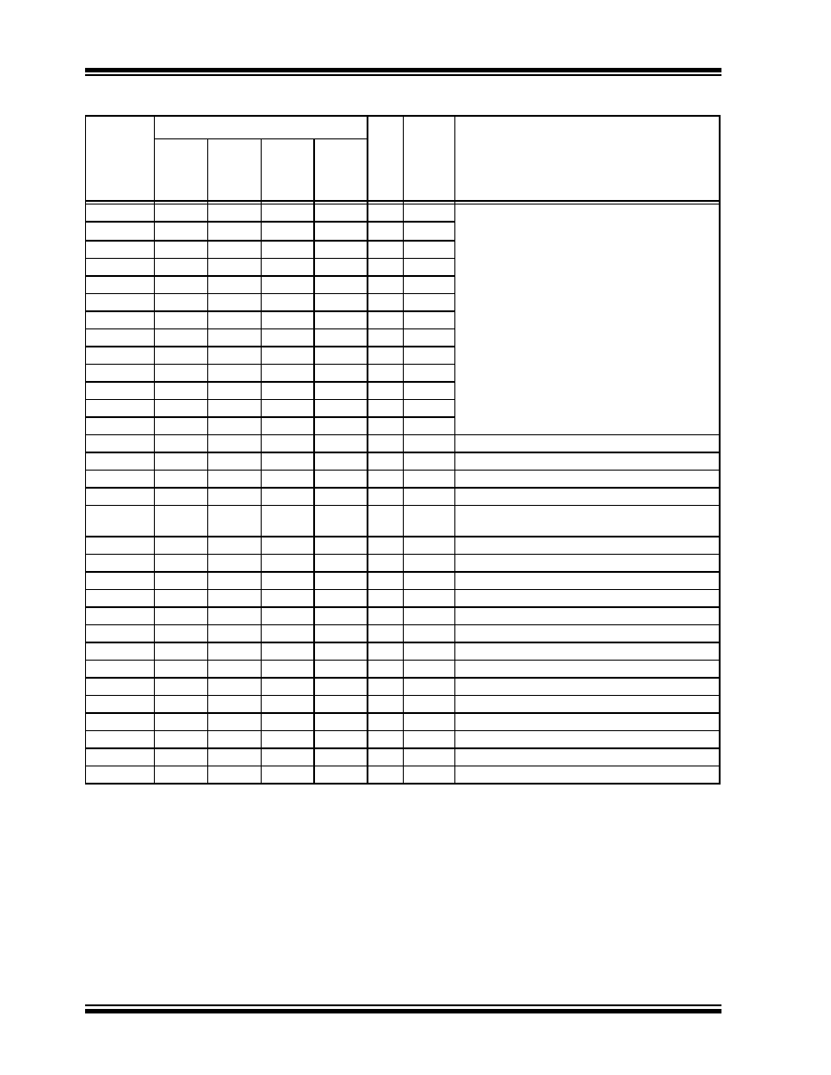
TABLE 1-4:
PIC24F16KL40X/30X FAMILY PINOUT DESCRIPTIONS
Function
Pin Number
I/O
Buffer
Description
20-Pin
PDIP/
SSOP/
SOIC
20-Pin
QFN
28-Pin
SPDIP/
SSOP/
SOIC
28-Pin
QFN
AN0
2
19
2
27
I
ANA
A/D Analog Inputs. Not available on PIC24F16KL30X
family devices.
AN1
3
20
3
28
I
ANA
AN2
4141
I
ANA
AN3
5252
I
ANA
AN4
6363
I
ANA
AN5
—
7
4
I
ANA
AN9
18
15
26
23
I
ANA
AN10
17
14
25
22
I
ANA
AN11
16
13
24
21
I
ANA
AN12
15
12
23
20
I
ANA
AN13
7496
I
ANA
AN14
8
5
10
7
I
ANA
AN15
9
6
11
8
I
ANA
ASCL1
—
15
12
I/O
I2C
Alternate MSSP1 I2C Clock Input/Output
ASDA1
—
14
11
I/O
I2C
Alternate MSSP1 I2C Data Input/Output
AVDD
20
17
28
25
I
ANA
Positive Supply for Analog modules
AVSS
19
16
27
24
I
ANA
Ground Reference for Analog modules
CCP1
14
11
20
17
I/O
ST
CCP1/ECCP1 Capture Input/Compare and PWM
Output
CCP2
15
12
23
20
I/O
ST
CCP2 Capture Input/Compare and PWM Output
CCP3
13
10
19
16
I/O
ST
CCP3 Capture Input/Compare and PWM Output
C1INA
8574
I
ANA
Comparator 1 Input A (+)
C1INB
7463
I
ANA
Comparator 1 Input B (-)
C1INC
5252
I
ANA
Comparator 1 Input C (+)
C1IND
4141
I
ANA
Comparator 1 Input D (-)
C1OUT
17
14
25
22
O
—
Comparator 1 Output
C2INA
5252
I
ANA
Comparator 2 Input A (+)
C2INB
4141
I
ANA
Comparator 2 Input B (-)
C2INC
8574
I
ANA
Comparator 2 Input C (+)
C2IND
7463
I
ANA
Comparator 2 Input D (-)
C2OUT
14
11
20
17
O
—
Comparator 2 Output
CLK I
7496
I
ANA
Main Clock Input
CLKO
8
5
10
7
O
—
System Clock Output
Legend:
TTL = TTL input buffer
ST = Schmitt Trigger input buffer
ANA = Analog level input/output
I2C = I2C/SMBus input buffer
发布紧急采购,3分钟左右您将得到回复。
相关PDF资料
PIC16F689-I/SO
IC PIC MCU FLASH 4KX14 20SOIC
PIC16F689-I/ML
IC PIC MCU FLASH 4KX14 20QFN
PIC16F685-I/SO
IC PIC MCU FLASH 4KX14 20SOIC
PIC16F886-I/SO
IC PIC MCU FLASH 8KX14 28SOIC
PIC18LF6680T-I/L
IC PIC MCU FLASH 32KX16 68PLCC
PIC16C54C-20I/SS
IC MCU OTP 512X12 20SSOP
PIC16C621A-20/P
IC MCU OTP 1KX14 COMP 18DIP
PIC18F4439-E/P
IC PIC MCU FLASH 6KX16 40DIP
相关代理商/技术参数
PIC24F08KL401T-I/MQ
功能描述:16位微控制器 - MCU 8KB FLASH 1KB RAM 512B 3V 10-BIT ADC RoHS:否 制造商:Texas Instruments 核心:RISC 处理器系列:MSP430FR572x 数据总线宽度:16 bit 最大时钟频率:24 MHz 程序存储器大小:8 KB 数据 RAM 大小:1 KB 片上 ADC:Yes 工作电源电压:2 V to 3.6 V 工作温度范围:- 40 C to + 85 C 封装 / 箱体:VQFN-40 安装风格:SMD/SMT
PIC24F08KL401T-I/SO
功能描述:16位微控制器 - MCU 8KB FLASH 1KB RAM 512B 3V 10-BIT ADC RoHS:否 制造商:Texas Instruments 核心:RISC 处理器系列:MSP430FR572x 数据总线宽度:16 bit 最大时钟频率:24 MHz 程序存储器大小:8 KB 数据 RAM 大小:1 KB 片上 ADC:Yes 工作电源电压:2 V to 3.6 V 工作温度范围:- 40 C to + 85 C 封装 / 箱体:VQFN-40 安装风格:SMD/SMT
PIC24F08KL401T-I/SS
功能描述:16位微控制器 - MCU 8KB FLASH 1KB RAM 512B 3V 10-BIT ADC RoHS:否 制造商:Texas Instruments 核心:RISC 处理器系列:MSP430FR572x 数据总线宽度:16 bit 最大时钟频率:24 MHz 程序存储器大小:8 KB 数据 RAM 大小:1 KB 片上 ADC:Yes 工作电源电压:2 V to 3.6 V 工作温度范围:- 40 C to + 85 C 封装 / 箱体:VQFN-40 安装风格:SMD/SMT
PIC24F08KL402
制造商:MICROCHIP 制造商全称:Microchip Technology 功能描述:Low-Power, Low-Cost, General Purpose 16-Bit Flash Microcontrollers with nanoWatt XLP Technology
PIC24F08KL402-I/ML
功能描述:16位微控制器 - MCU 8KB FLASH 1KB RAM 512B 3V 10-BIT ADC RoHS:否 制造商:Texas Instruments 核心:RISC 处理器系列:MSP430FR572x 数据总线宽度:16 bit 最大时钟频率:24 MHz 程序存储器大小:8 KB 数据 RAM 大小:1 KB 片上 ADC:Yes 工作电源电压:2 V to 3.6 V 工作温度范围:- 40 C to + 85 C 封装 / 箱体:VQFN-40 安装风格:SMD/SMT
PIC24F08KL402-I/MQ
功能描述:16位微控制器 - MCU 8KB FL 1KB RAM 512B 3V 10-bit ADC RoHS:否 制造商:Texas Instruments 核心:RISC 处理器系列:MSP430FR572x 数据总线宽度:16 bit 最大时钟频率:24 MHz 程序存储器大小:8 KB 数据 RAM 大小:1 KB 片上 ADC:Yes 工作电源电压:2 V to 3.6 V 工作温度范围:- 40 C to + 85 C 封装 / 箱体:VQFN-40 安装风格:SMD/SMT
PIC24F08KL402-I/SO
功能描述:16位微控制器 - MCU 8KB FLASH 1KB RAM 512B 3V 10-BIT ADC RoHS:否 制造商:Texas Instruments 核心:RISC 处理器系列:MSP430FR572x 数据总线宽度:16 bit 最大时钟频率:24 MHz 程序存储器大小:8 KB 数据 RAM 大小:1 KB 片上 ADC:Yes 工作电源电压:2 V to 3.6 V 工作温度范围:- 40 C to + 85 C 封装 / 箱体:VQFN-40 安装风格:SMD/SMT
PIC24F08KL402-I/SP
功能描述:16位微控制器 - MCU 8KB FLASH 1KB RAM 512B 3V 10-BIT ADC RoHS:否 制造商:Texas Instruments 核心:RISC 处理器系列:MSP430FR572x 数据总线宽度:16 bit 最大时钟频率:24 MHz 程序存储器大小:8 KB 数据 RAM 大小:1 KB 片上 ADC:Yes 工作电源电压:2 V to 3.6 V 工作温度范围:- 40 C to + 85 C 封装 / 箱体:VQFN-40 安装风格:SMD/SMT